Add to Cart
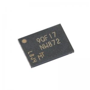
MT29F1G01ABAFDWB-IT:F NAND Flash memory ic chip SLC 1Gbit 1GX1 UPDFN 35 mA UPDFN-8
Specifications
| Product Attribute | Attribute Value |
|---|---|
| SMD/SMT | |
| U-PDFN-8 | |
| 1 Gbit | |
| FBGA Code | NW872 |
| 1 G x 1 | |
| Asynchronous | |
| 1 bit | |
| 2.7 V | |
| 3.6 V | |
| 35 mA | |
| - 40 C | |
| + 85 C | |
| Maximum Clock Frequency: | 133 MHz |
Description
Serial peripheral interface (SPI) NAND is an SLC NAND Flash memory device that provides a cost-effective
nonvolatile memory storage solution where pin count must be kept to a minimum. It is also an alternative
solution to SPI NOR, offering superior write performance and cost per bit over SPI NOR.
The hardware interface creates a low pin-count device with a standard pinout that remains the same from
one density to another and supports future upgrades to higher densities without board redesign.
The serial electrical interface follows the industry-standard serial peripheral interface. New command
protocols and registers are defined for SPI operation. The command set resembles common SPI-NOR
command sets, modified to handle NAND specific functions and additional new features.

Features
• Single-level cell (SLC) technology
• 1Gb density
• Organization
– Page size x1: 2176 bytes (2048 + 128 bytes)
– Block size: 64 pages (128K + 8K bytes)
– Plane size: 1Gb (1 plane, 1024 blocks per plane)
• Standard and extended SPI-compatible serial bus in-terface
– Instruction, address on 1 pin; data out on 1, 2, or 4 pins
– Instruction on 1 pin; address, data out on 2 or 4 pins
– Instruction, address on 1 pin; data in on 1 or 4 pins
• Device initialization
– Automatic device initialization after power-up
• Security
– Blocks 7:0 are valid when shipped from factory with ECC enabled
– Software write protection with lock register
– Hardware write protection to freeze BP bits
– Lock tight to freeze BP bits during one power cycle
• Permanent block lock protection – OTP Space: 10 pages one-time programmable NAND Flash memory area
• Operating voltage range
– VCC = 2.7–3.6V
• Operating temperature
– Industrial: –40°C to +85°C
• Quality and reliability – Data retention: JESD47H-compliant; see qualification report
– Additional: Uncycled data retention: 10 years 24/7 @85°C
– Endurance: 100,000 PROGRAM/ERASE cycles • Package
– 6-pin SOP, 300 mils
– 8-pin U-PDFN, 8mm x 6mm x 0.65mm (MLP8)
– 24-ball T-PBGA, 05/6mm x 8mm (5 x 5 array)
Trading Guides
| Shipping | Delivery period | For in-stock parts, orders are estimated to ship out in 3 days. |
| Shipping rates | After confirming the order, we will evaluate the shipping cost based on the weight of the goods | |
| Shipping option | We provide DHL, FedEx, EMS, SF Express, and Registered Air Mail international shipping. | |
| Shipping tracking | We will notify you by email with tracking number once order is shipped. | |
| Returning warranty | Returning | Returns are normally accepted when completed within 30 days from date of shipment.Parts should be unused and in original packaging.Customer has to take charge for the shipping. |
| Warranty | All Retechip purchases come with a 30-day money-back return policy, This warranty shall not apply to any item where defects have been caused by improper customer assembly, failure by customer to follow instructions, product modification, negligent or improper operation | |
| Ordering |
Payment
| T/T,PayPal, Credit Card includes Visa, Master, American Express. |